 | –≠–ª–µ–∫—Ç—Ä–æ–Ω–Ω—ã–π –∫–æ–º–ø–æ–Ω–µ–Ω—Ç: LTC3411 | –°–∫–∞—á–∞—Ç—å:  PDF PDF  ZIP ZIP |
1
LTC3445
3445fa
Buck Regulator
High Efficiency: Up to 93%
600mA Output Current (V
CC1
= 3V, V
OUT
= 1.3V)
Programmable Output Voltage: 0.85V to 1.55V
2.5V to 5.5V Input Voltage Range
1.5MHz Constant Frequency or Spread Spectrum
Option
Soft-Start
LDOs
Two LDO Regulators: 0.3V Dropout at 50mA
PowerPath Controller
Dynamically Regulates V
CC
BATT
I
2
C
Standard (100kHz) or Fast Mode (400kHz)
24-Lead (4mm
◊ 4mm) QFN Package
I
2
C Controllable
Buck Regulator with Two LDOs
in a 4mm
◊ 4mm QFN
Intel's Microprocessor Supply (PXA27X)
Portable Instruments
, LTC and LT are registered trademarks of Linear Technology Corporation.
The LTC
Æ
3445 contains a high efficiency monolithic syn-
chronous current mode buck regulator, two LDO regula-
tors, a PowerPath
TM
controller and an I
2
C
TM
interface.
The buck regulator has a 6-bit programmable output range
of 0.85V to 1.55V. Also, the buck regulator uses either a
constant (1.5MHz) or a spread spectrum switching fre-
quency. Using the spread spectrum option allows for a
lower noise regulated output as well as low noise at the
input. In addition, the regulated output voltage slew rate is
programmable via the I
2
C interface.
The LTC3445 contains two LDO voltage regulators. The
regulator output voltages are externally resistor program-
mable. Each LDO is capable of delivering up to 50mA.
The LTC3445 contains control circuitry (PowerPath) for
automatic back-up battery selection. V
BACKUP
is typically
a coin cell.
Typical supply current during operation is only 360
µA and
drops to 27
µA in shutdown. The 2.5V to 5.5V input
voltage range makes the LTC3445 ideal for single Li-Ion
battery-powered applications. Automatic Burst Mode
Æ
operation increases efficiency at light loads, further ex-
tending battery life.
Burst Mode is a registered trademark of Linear Technology Corporation.
PowerPath is a trademark of Linear Technology Corporation.
I
2
C is a trademark of Philips Electronics N.V.
Protected by U.S. Patents, including 5481178, 6580258, 6304066, 6127815, 6498466,
6611131, Spread Spectrum patent pending.
FEATURES
DESCRIPTIO
U
APPLICATIO S
U
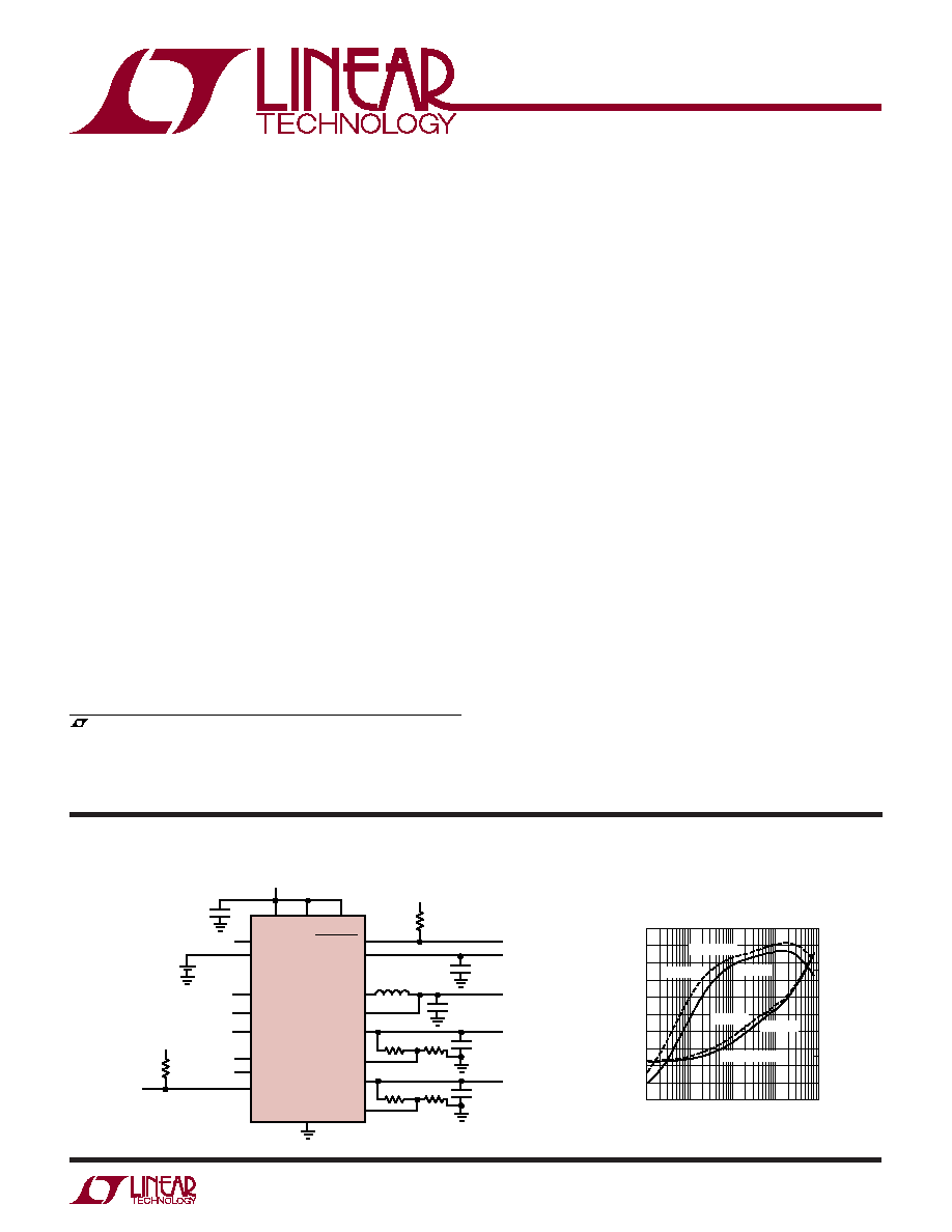
TYPICAL APPLICATIO
U
+
2.2
µH
705k
604k
4.7
µF
CER
4.7
µF
CER
10
µF
CER
1.3V
0.85V
TO 1.55V
3V
TYP
V
CC2
GND
LTC3445
V
CC1
nBATT_FAULT
V
CC1
BATTFAULT
4.7
µF
CER
V
CC
BATT
V
TRACK
3V
COIN
CELL
V
BACKUP
LDO1
LDO1FB
LDO2
LDO2FB
SW
FB
RUN
SDA
I
2
C BUS
PWR_EN
V
CC1
OR GND
V
CC1
OR GND
SCL
ADD7
ADD6
PGOOD
V
CC
nV
CC
_FAULT
V
CC
20k
3445 TA01
503k
604k
10
µF
CER
1.1V
V
BACKUP
20k
V
BACKUP
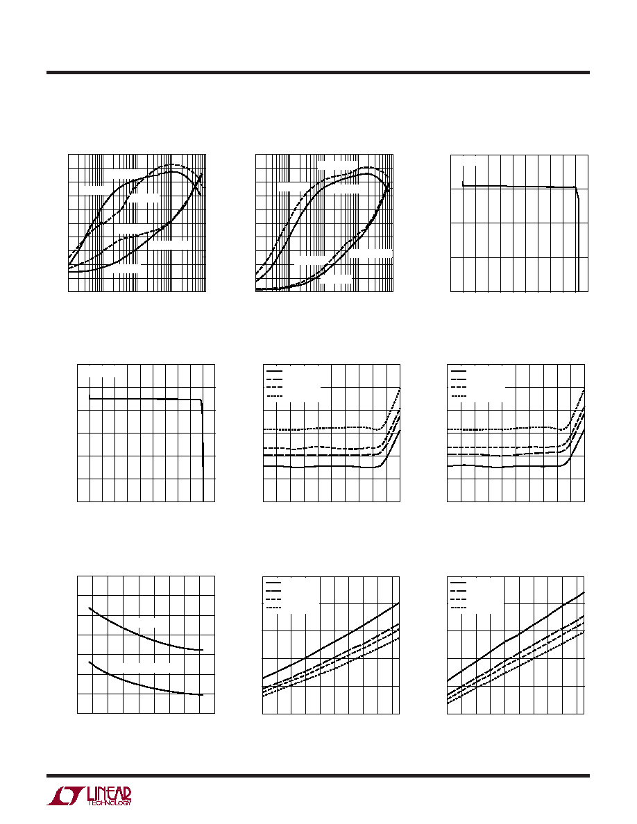
Efficiency and Power Loss
vs Load Current, V
CC1
= 3.6V
LOAD CURRENT (mA)
30
EFFICIENCY (%)
POWER LOSS (mW)
90
100
20
10
80
50
70
60
40
0.1
10
100
1000
3445 TA01b
0
1
DAC MAX
DAC MIN
DAC MIN
DAC MAX
100
1000
10
1.0
0.1
EFFICIENCY
POWER LOSS
2
LTC3445
3445fa
Order Options Tape and Reel: Add #TR
Lead Free: Add #PBF Lead Free Tape and Reel: Add #TRPBF
Lead Free Part Marking:
http://www.linear.com/leadfree/
ORDER PART NUMBER
(Note 1)
ABSOLUTE AXI U RATI GS
W
W
W
U
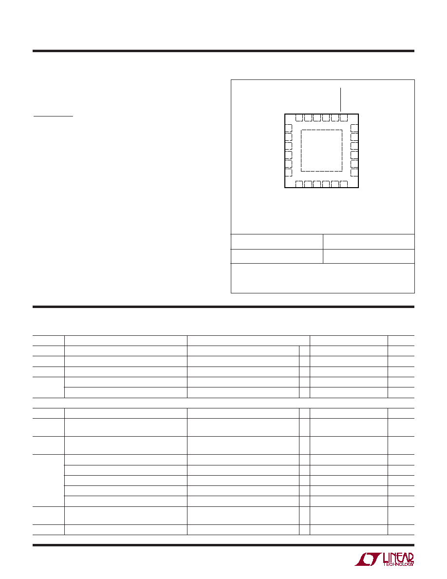
PACKAGE/ORDER I FOR ATIO
U
U
W
Consult LTC Marketing for parts specified with wider operating temperature ranges.
LTC3445EUF
T
JMAX
= 125
∞C,
JA
= 37
∞C/W,
JC
= 2.6
∞C/W
EXPOSED PAD (PIN 25) IS GND, MUST BE SOLDERED TO PCB
24 23 22 21 20 19
7
8
9
TOP VIEW
25
UF PACKAGE
24-LEAD (4mm
◊ 4mm) PLASTIC QFN
10 11 12
6
5
4
3
2
1
13
14
15
16
17
18
V
TRACK
V
BACKUP
V
CC1
PGOOD
ADD7
SDA
V
CC
BATT
FB
NC
RUN
SW
NC
LDO2FB
LDO2
V
CC2
LDO1
LDO1FB
BATTFAULT
NC
SCL
ADD6
V
CC1
GND
NC
The
denotes the specifications which apply over the full operating
temperature range, otherwise specifications are at T
A
= 25
∞C. V
CC1
= V
CC2
= 3.6V, unless otherwise noted.
ELECTRICAL CHARACTERISTICS
UF PART MARKING
3445
V
CC1
, V
CC2
, SDA, SCL Voltages .................. ≠ 0.3V to 6V
RUN, V
TRACK
, V
BACKUP
, PGOOD, ADD7,
ADD6, FB, V
CC
BATT,
BATTFAULT Voltages .............................. ≠ 0.3V to V
CC1
SW Voltage ................................ ≠ 0.3V to (V
CC1
+ 0.3V)
LDO1FB, LDO2FB Voltages ..................... ≠ 0.3V to V
CC2
LDO1, LDO2 Voltages ................ ≠ 0.3V to (V
CC2
+ 0.3V)
LDO1, LDO2 Source Current ............................... 50mA
V
CC
BATT Source Current ...................................... 8mA
P-Channel Switch Source Current (DC) ............. 800mA
N-Channel Switch Sink Current (DC) ................. 800mA
Peak SW Sink and Source Current ........................ 1.3A
LDO1, LDO2, V
CC
BATT Output Short-Circuit
Duration .......................................................... Indefinite
Operating Temperature Range (Note 2) ...≠40
∞C to 85∞C
Junction Temperature (Note 3) ............................ 125
∞C
Storage Temperature Range ................. ≠65
∞C to 125∞C
SYMBOL
PARAMETER
CONDITIONS
MIN
TYP
MAX
UNITS
V
CC1,
V
CC2
Input Voltage Range
2.5
5.5
V
RUN
Run Threshold
0.3
1
1.5
V
PGOOD
Reports Undervoltage of any Regulator
PGOOD = 0.4V
3
mA
I
S
DC Bias Current (Shutdown)
RUN = 0
27
50
µA
DC Bias Current (Buck, LDO1, LDO2 Disabled)
RUN = V
CC1
105
150
µA
Buck Regulator
R
FB
Feedback Resistance
340
k
V
OUT(MIN)
Regulated Output Voltage
I
OUT
= 100mA, Burst Mode Operation
0.824
0.850
0.875
V
Disabled
V
OUT(MAX)
Regulated Output Voltage
I
OUT
= 100mA, Burst Mode Operation
1.504
1.55
1.597
V
Disabled
V
OUT(STEP)
Output Voltage Step Size (0 to 48)
I
OUT
= 100mA
13.1
14.7
16.1
mV
Output Voltage Slew Rate = 00
I
OUT
= 100mA, V
OUT
= 0.85V to 1.55V
11.3
mV/
µs
Output Voltage Slew Rate = 01
I
OUT
= 100mA, V
OUT
= 0.85V to 1.55V
7.5
mV/
µs
Output Voltage Slew Rate = 10
I
OUT
= 100mA, V
OUT
= 0.85V to 1.55V
3.8
mV/
µs
Output Voltage Slew Rate = 11
I
OUT
= 100mA, V
OUT
= 0.85V to 1.55V
0.9
mV/
µs
I
PK
Peak Inductor Current
V
CC1
= 3V, V
FB
= 0.5V or V
OUT
= 90%,
0.75
1
1.25
A
Duty Cycle < 35%
V
LOADREG
Output Voltage Load Regulation
0.5
%
3
LTC3445
3445fa
The
denotes the specifications which apply over the full operating
temperature range, otherwise specifications are at T
A
= 25
∞C. V
CC1
= V
CC2
= 3.6V, unless otherwise noted.
ELECTRICAL CHARACTERISTICS
SYMBOL
PARAMETER
CONDITIONS
MIN
TYP
MAX
UNITS
I
S
Additional Input DC Bias Current For Buck (Note 4)
Active Mode
V
OUT
= 90%, I
LOAD
= 0A
220
µA
Sleep Mode
V
OUT
= 103%, I
LOAD
= 0A
6
µA
f
OSC
Nominal Oscillator Frequency
V
OUT
= 100%
1.2
1.5
1.8
MHz
V
OUT
= 0V
300
kHz
R
PFET
R
DS(ON)
of P-Channel FET
I
SW
= 100mA
0.45
R
NFET
R
DS(ON)
of N-Channel FET
I
SW
= ≠100mA
0.325
I
LSW
SW Leakage
V
RUN
= 0V, V
SW
= 0V or 5V, V
CC1
= 5V
1
µA
LDO1
I
S
Additional DC Bias for LDO1
23
30
µA
V
OUT
Regulated Output Voltage
2.5V < V
IN
< 5.5V, 1mA < I
LOAD
< 50mA
0.582
V
CC2
≠
V
0.3
Line Regulation
V
CC2
= 2.5V to 5.5V, I
LOAD
= 1mA, V
OUT
= 1.2V
1
5
mV
Load Regulation
V
CC2
= 2.5V,
I
LOAD
= 1mA to 50mA, V
OUT
= 1.2V
15
mV
Dropout Voltage
I
LOAD
= 50mA
0.3
V
V
FB
LDO Feedback Voltage
I
LOAD
= 0mA
0.582
0.6
0.618
V
LDO2
I
S
Additional DC Bias for LDO2
23
30
µA
V
OUT
Regulated Output Voltage
2.5V < V
IN
< 5.5V, 1mA < I
LOAD
< 50mA
0.582
V
CC2
≠
V
0.3
Line Regulation
V
CC2
= 2.5V to 5.5V, I
LOAD
= 1mA, V
OUT
= 1.2V
1
5
mV
Load Regulation
V
CC2
= 2.5V,
I
LOAD
= 1mA to 50mA, V
OUT
= 1.2V
15
mV
Dropout Voltage
I
LOAD
= 50mA
0.3
V
V
FB
LDO Feedback Voltage
I
LOAD
= 0mA
0.582
0.6
0.618
V
PowerPath Controller
V
TRACK
Tracked Input Voltage
3
V
CC1
≠
V
0.2
V
TRACK
≠
Tracked Output Voltage at V
CC
BATT
3V < V
TRACK
< V
CC1
≠ 0.2V
≠0.2
0
0.2
V
V
CC
BATT
V
BACKUP
Backup Battery Voltage
2
5.5
V
I
BACKUP
Backup Battery Bias Current
V
CC1
= V
TRACK
= 0V, V
BACKUP
= 2.5V
4
6.5
µA
V
CC
BATT
V
CC
BATT Output
V
TRACK
= 0V, V
CC1
= 4V, I
VCCBAT
= 8mA
2.85
3
3.1
V
I
VCCBATT
Max V
CC
BATT Output Current
V
CC1
= 2.5V
8
mA
BATTFAULT V
CC1
High Level (Good)
Where BATTFAULT Goes High
2.65
2.8
2.9
V
V
CC1
Low Level (Bad)
Where BATTFAULT Goes Low
2.4
2.5
2.6
V
Hysteresis
V
CC1
= 0V to 4.2V, 4.2 to 0V
0.3
V
I
2
C Interface
f
I2C(MAX)
Maximum I
2
C Operating Frequency
(Note 5)
400
kHz
t
BUF
Bus Free Time Between Stop and Start
(Note 5)
1.3
µs
Condition
t
HD(RSTA)
Hold Time After (Repeated)
(Note 5)
600
ns
Start Condition
4
LTC3445
3445fa
Note 1: Absolute Maximum Ratings are those values beyond which the life
of a device may be impaired.
Note 2: The LTC3445EUF is guaranteed to meet performance specifica-
tions from 0
∞C to 70∞C. Specifications over the ≠40∞C to 85∞C operating
temperature range are assured by design, characterization and correlation
with statistical process controls.
ELECTRICAL CHARACTERISTICS
Note 3: T
J
is calculated from the ambient temperature, T
A
, and power
dissipation, P
D
, according to the following formula:
T
J
= T
A
+ P
D
∑ 37
∞C/W
Note 4: Dynamic supply current is higher due to the gate charge being
delivered at the switching frequency.
Note 5: Determined by design, not production tested.
The
denotes the specifications which apply over the full operating
temperature range, otherwise specifications are at T
A
= 25
∞C. V
CC1
= V
CC2
= 3.6V, unless otherwise noted.
ELECTRICAL CHARACTERISTICS
SYMBOL
PARAMETER
CONDITIONS
MIN
TYP
MAX
UNITS
t
SU(RSTA)
Repeated Start Condition Setup Time
(Note 5)
600
ns
t
SU(STOP)
Stop Condition Setup Time
(Note 5)
600
ns
t
HD(DIN)
Data Hold Time, Input
(Note 5)
0
ns
t
SU(DAT)
Data Setup Time
(Note 5)
100
ns
V
THR
SCL and SDA Logic Input Threshold
1.8
V
V
HYS
SCL and SDA Logic Input Hysteresis
(Note 5)
50
mV
I
LVTRACK
V
TRACK
Leakage
V
CC
= 3.6V
1.44
2.2
µA
I
LVBACKUP
V
BACKUP
Leakage
V
CC
= 3.6V
1
µA
I
LADD7
ADD7 Leakage
V
CC
= 3.6V
1
µA
I
LADD6
ADD6 Leakage
V
CC
= 3.6V
1
µA
I
LSCL
SCL Leakage
V
CC
= 3.6V
1
µA
I
LSDA
SCL Leakage
V
CC
= 3.6V
1
µA
I
LLDO1
LDO1 Leakage
V
CC
= 3.6V, RUN = 0
1
µA
I
LLDO2
LDO2 Leakage
V
CC
= 3.6V, RUN = 0
1
µA
I
LLDO1FB
LDO1FB Leakage
V
CC
= 3.6V, RUN = 0
1
µA
I
LLDO2FB
LDO2FB Leakage
V
CC
= 3.6V, RUN = 0
1
µA
I
LBATTFAULT
BATTFAULT Leakage
V
CC
= 3.6V
1
µA
I
FB1,2
LDO Feedback Input Current
V
FB1
= 0.6V
1
µA
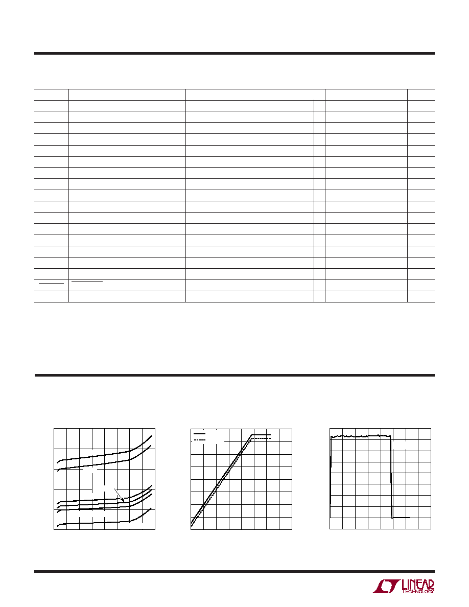
TYPICAL PERFOR A CE CHARACTERISTICS
U
W
Supply Current vs Supply Voltage
SUPPLY VOLTAGE (V)
2.4
SUPPLY CURRENT (
µ
A)
300
400
500
3.6
4.4
5.6
3445 G01
200
100
0
2.8
3.2
4
4.8
5.2
ALL ON
BUCK
TWO LDOs
RUN = HIGH
RUN = LOW
ONE LDO
V
OUT
vs DAC
DAC VALUE
0
V
OUT
(V)
1.2
1.4
80
3445 G02
1.0
0.8
20
40
60
10
30
50
70
1.6
1.1
1.3
0.9
1.5
0mA
600mA
DAC VALUE
0
V
OUT(N)
≠ V
OUT(N≠1)
(V)
0.008
0.010
0.012
80
3445 G03
0.006
0.004
≠0.002
20
40
60
10
30
50
70
0.002
0
0.016
0.014
100mA
V
OUT
Step Size vs DAC
5
LTC3445
3445fa
Buck Efficiency and Power Loss
vs Load Current, V
CC1
= 2.5V
Buck Output Voltage
vs Load Current
LOAD CURRENT (mA)
30
EFFICIENCY (%)
POWER LOSS (mW)
90
100
20
10
80
50
70
60
40
0.1
10
100
1000
3445 G04
0
1
100
1000
10
1.0
0.1
DAC MAX
DAC MIN
DAC MIN
DAC MAX
EFFICIENCY
POWER LOSS
LOAD CURRENT (mA)
30
EFFICIENCY (%)
POWER LOSS (mW)
90
100
20
10
80
50
70
60
40
0.1
10
100
1000
3445 G05
0
1
100
1000
10
1.0
0.1
DAC MAX
DAC MIN
DAC MIN
DAC MAX
EFFICIENCY
POWER LOSS
LOAD CURRENT (mA)
≠100
BUCK OUTPUT (V)
0.800
0.850
700
3445 G06
0.750
0.700
100
300
0.900
500
900
DAC = MIN
Buck Output Voltage
vs Load Current
I
VCC2
vs Temperature (RUN = V
CC1
)
LOAD CURRENT (mA)
≠100
BUCK OUTPUT (V) 1.500
1.540
1.520
1.560
700
3445 G07
1.480
1.460
100
300
1.580
500
900
DAC = MAX
TEMPERATURE (
∞C)
0
V
CC2
LEAKAGE CURRENT (
µ
A)
0.4
0.8
1.2
0.2
0.6
1.0
≠10
30
70
110
3445 G08
150
≠50
V
CC2
= 2.5V
V
CC2
= 3.6V
V
CC2
= 4.2V
V
CC2
= 5.5V
I
VCC2
vs Temperature (RUN = 0V)
TEMPERATURE (
∞C)
0
V
CC2
LEAKAGE CURRENT (
µ
A)
0.4
0.8
1.2
0.2
0.6
1.0
≠10
30
70
110
3445 G09
150
≠50
V
CC2
= 2.5V
V
CC2
= 3.6V
V
CC2
= 4.2V
V
CC2
= 5.5V
TYPICAL PERFOR A CE CHARACTERISTICS
U
W
R
DS(ON)
vs Input Voltage
Synchronous Switch R
DS(ON)
vs Temperature
INPUT VOLTAGE (V)
2.2 2.6
3
3.4 3.8 4.2 4.6
5
5.4
250
R
DS(ON)
(m
)
300
400
450
500
600
3445 G10
350
5.8
550
MAIN SWITCH
SYNCHRONOUS SWITCH
TEMPERATURE (
∞C)
≠40
R
DS(ON)
(m
)
500
600
700
120
3445 G11
400
300
200
≠20
0
20
40
60
80 100
140
V
CC1
= 2.5V
V
CC1
= 3.6V
V
CC1
= 4.2V
V
CC1
= 5.5V
Main Switch R
DS(ON)
vs Temperature
TEMPERATURE (
∞C)
≠40
R
DS(ON)
(m
)
600
700
800
120
3445 G12
500
400
300
≠20
0
20
40
60
80 100
140
V
CC1
= 2.5V
V
CC1
= 3.6V
V
CC1
= 4.2V
V
CC1
= 5.5V
Buck Efficiency and Power Loss
vs Load Current, V
CC1
= 4.2V
6
LTC3445
3445fa
TYPICAL PERFOR A CE CHARACTERISTICS
U
W
Slew Rates DAC Min to DAC Max
Buck (DAC = Min)
100mA to 300mA Load Step
Buck Switching Frequency
vs V
CC1
Buck (DAC = Max)
100mA to 400mA Load Step
BUCK
VOLTAGE
50mV/DIV
LOAD
CURRENT
100mA/DIV
100
µs/DIV
3445 G13
20
µs/DIV
3445 G14
20
µs/DIV
3445 G15
Buck Switching Frequency
vs Temperature
Soft-Start (DAC = Min and Max)
4.7
Load
BUCK
OUTPUTS
500mV/DIV
200
µs/DIV
3445 G18
200mV/DIV
BUCK
VOLTAGE
50mV/DIV
LOAD
CURRENT
100mA/DIV
2.5
1.40
SWITCHING FREQUENCY (MHz) 1.44
1.48
1.52
1.56
1.60
3.5
4.5
3445 G16
5.5
V
CC1
(V)
TEMPERATURE (
∞C)
≠50
1.460
1.440
SWITCHING FREQUENCY (MHz)
1.480
1.500
0
50
100
150
3445 G17
1.520
1.540
1.560
≠25
25
75
125
V
CC
BATT vs V
CC1
PowerPath LDO Load Step
1mA to 5.5mA
V
CC1
RAMP (V)
0
0
VOLTAGE (V)
1
2
3
V
CC1
4
3445 G19
5
6
V
TRACK
= V
BACKUP
= 2V
V
CC
BATT
V
CC
BATT vs V
TRACK
V
TRACK
RAMP (V)
0
0
VOLTAGE (V)
1
2
3
4
3445 G20
5
6
V
CC1
= 5.5V
V
BACKUP
= 2V
V
CC
BATT
0mA
5mA
V
TRACK
V
CC
BATT
20mV/DIV
LOAD
CURRENT
10mA/DIV
200
µs/DIV
3445 G21
7
LTC3445
3445fa
TYPICAL PERFOR A CE CHARACTERISTICS
U
W
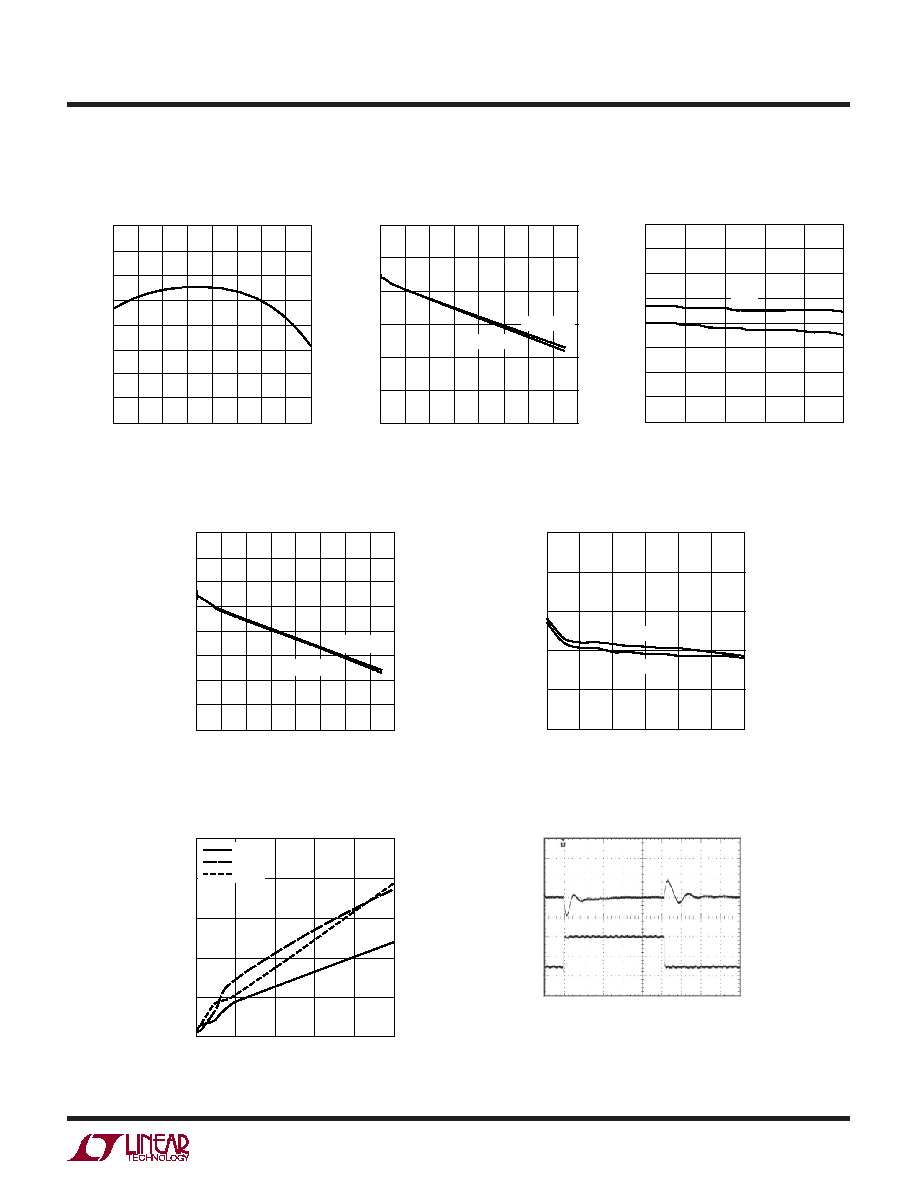
LDO Reference Voltage
vs Temperature
LDO Reference Voltage
vs Load Current
TEMPERATURE (
∞C)
≠50
LDO REFERENCE VOLTAGE (V)
0.598
25
3445 G22
0.596
≠25
0
150
50
0mA
75
100 125
0.594
0.592
0.590
0.498
0.600
0.602
0.604
LOAD CURRENT (mA)
0
LDO REFERENCE VOLTAGE (V)
0.604
0.606
0.608
30
50
80
3445 G23
0.602
0.600
0.598
0.596
10
20
40
60
70
V
CC2
= 2.5V
V
CC2
= 5.5V
LDO Output Voltage vs V
CC2
V
CC2
(V)
2.5
LDO OUTPUT VOLTAGE (V)
1.197
1.198
1.199
4.3
5.5
3445 G24
1.196
1.195
1.194
3.1
3.7
4.9
1.200
1.201
1.202
10mA
50mA
LDO Output Voltage
vs Load Current
LDO Output Voltage
vs Load Current
LOAD CURRENT (mA)
0
2.578
2.576
2.574
LDO OUTPUT VOLTAGE (V)
2.580
2.582
2.584
2.586
2.588
2.590
10
20
30
40
3445 G25
50
60
70
80
V
CC2
= 3.6V
V
CC2
= 5.5V
LOAD CURRENT (mA)
0
LDO OUTPUT VOLTAGE (V)
1.194
1.196
1.198
1.200
1.202
1.204
10
20
30
40
3445 G26
50
60
V
CC2
= 5.5V
V
CC2
= 2.5V
LDO Dropout Voltage
vs Load Current
LDO Load Step (10mA to 40mA)
LOAD CURRENT (mA)
0
LDO DROPOUT VOLTAGE (mV)
120
160
200
40
3445 G28
80
40
0
10
20
30
50
≠50
∞C
25
∞C
150
∞C
LDO
OUTPUT
20mV/DIV
LOAD
CURRENT
20mA/DIV
40
µs/DIV
3445 G29

8
LTC3445
3445fa
U
U
U
PI FU CTIO S
V
TRACK
(Pin 1): Supply Sense that V
CC
BATT Tracks when
above 3V. Must be
V
CC1
.
V
BACKUP
(Pin 2): Back-Up Battery Input.
V
CC1
(Pins 3, 10): Power Supply (2.5V to 5.5V). Both V
CC1
pins must be connected externally to the 2.5V to 5.5V
supply.
PGOOD (Pin 4): Fault Report (Undervoltage). Open-drain
driver sinks current whenever LDO1, LDO2 or buck out-
puts are low.
ADD7 (Pin 5): I
2
C Strappable Address (Bit 7)--V
CC1
or
ground.
SDA (Pin 6): I
2
C Data Input.
NC (Pin 7): Not Connected.
SCL (Pin 8): I
2
C Clock Input.
ADD6 (Pin 9): I
2
C Strappable Address (Bit 6)--V
CC1
or
ground.
GND (Pin 11): Buck NFET Ground.
NC (Pin 12): Not Connected.
NC (Pin 13): Not Connected.
SW (Pin 14): Buck Regulator Switch.
RUN (Pin 15): Chip Enable. 1.5V enables the part. Forcing
this pin below 0.3V shuts down the device. In shutdown,
all functions are disabled, drawing <35
µA supply current.
Do not leave RUN floating. Must be
V
CC1
.
NC (Pin 16): Not Connected.
FB (Pin 17): Buck Regulator Feedback.
V
CC
BATT (Pin 18): V
CC
BATT PowerPath Output.
BATTFAULT (Pin 19): Open-Drain Output. It is low when
V
CC1
is low.
LDO1FB (Pin 20): LDO1 Regulator Sense.
LDO1 (Pin 21): LDO1 Regulator Output.
V
CC2
(Pin 22): LDO Regulator Supply Voltage.
LDO2 (Pin 23): LDO2 Regulator Output.
LDO2FB (Pin 24): LDO2 Regulator Sense.
Exposed Pad (Pin 25): Ground. Must be soldered to PCB
ground for electrical contact and optimum thermal
performance.
9
LTC3445
3445fa
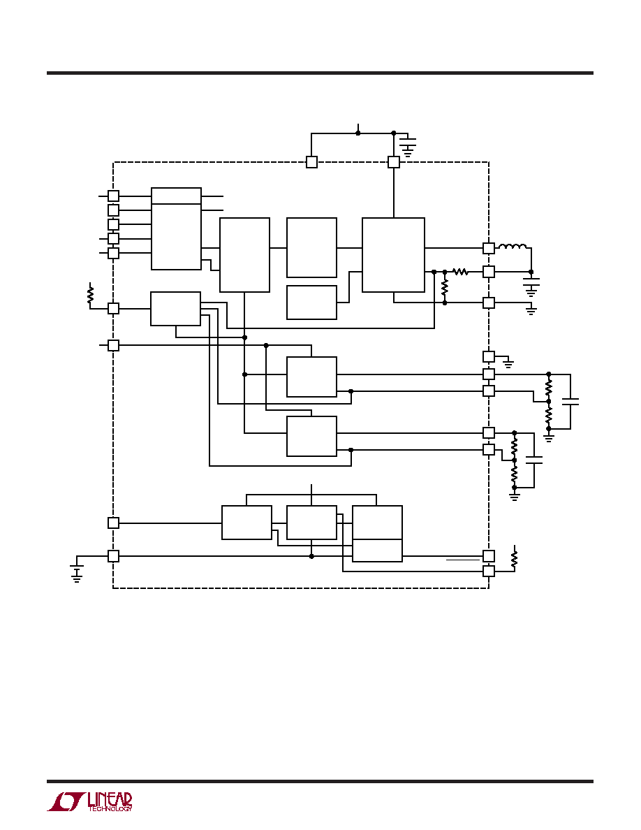
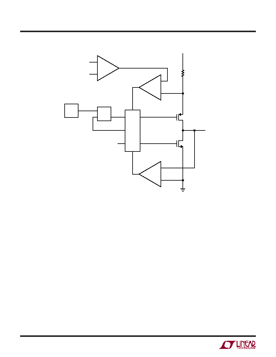
Figure 1
17
14
BUCK REGULATOR
V
REF
SW
OSC ADJUST
3445 F01
FB
SW
15
3
10
RUN
PWR_EN
V
CC1
OR GND
V
CC1
OR GND
6
SDA
8
SCL
5
ADD7
9
ADD6
4
22
PGOOD
V
CC
V
CC
V
CC2
1
V
TRACK
2
V
BACKUP
V
BACKUP
FB
11
GND
21
LDO1 OUT
25
EXPOSED PAD
20
LD01FB
23
LDO2 OUT
24
LD02FB
18
V
CC
BATT
V
BACKUP
19
BATTFAULT
C1
C
IN1
V
CC
C21
C11
R3
R4
GND
SOFT-START
V
CC1
POWER FOR ALL EXCEPT
LDOs AND BUCK PFET
SLEW
CONTROL
V
OUT
CONTROL
STRAPPABLE
STRAPPABLE
BUCK/LDO
ENABLE
BURST
V
REF
DAC
0.6V
SPREAD
SPECTRUM
PowerPath
CONTROL
PowerPath
LDO
POWER
SWITCH
DRIVER
POWER
SWITCH
LDO1
V
CC1
V
CC1
L1
REF
POWER FOR LDOs
OUT
FB
POWER
GOOD
R1
R2
LDO2
REF
OUT
FB
I
2
C
+
3V
COIN
CELL
FU CTIO AL DIAGRA S
U
U
W
10
LTC3445
3445fa
FU CTIO AL DIAGRA S
U
U
W
Figure 2. Buck Regulator Detail
V
FB
V
REF
EA
PEAK CURRENT LEVEL REFERENCE
BURST
R
S
SW
PFET
NFET
3445 F02
L
L
V
CC1
I
COMP
I
RCOMP
QB
Q
R
S
LOGIC
OSC
11
LTC3445
3445fa
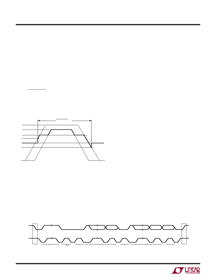
TI I G DIAGRA
U
W
W
t
BUF
t
SUSTO
3445 TD
t
HD(STA)
t
HD(DAT)
t
SU(STA)
t
SU(DAT)
t
LOW
t
HIGH
t
r
t
f
t
HD(STA)
SCL
SDA
START
CONDITION
REPEATED START
CONDITION
STOP
CONDITION
START
CONDITION
I
2
C Fast Mode Timing Specifications (for Reference)
SYMBOL
PARAMETER
MIN
TYP
MAX
UNITS
f
I2C(MAX)
Maximum I
2
C Operating Frequency
0
400
kHz
t
BUF
Bus Free Time Between Stop and Start Condition
1.3
µs
t
HD(RSTA)
Hold Time After (Repeated) Start Condition
0.6
µs
t
SU(RSTA)
Repeated Start Condition Setup Time
0.6
µs
t
SU(STOP)
Stop Condition Setup Time
0.6
µs
t
HD(DAT)
Data Hold Time
0
0.9
ns
t
SU(DAT)
Data Setup Time
100
ns
t
LOW
Clock Low Period
1.3
µs
t
HIGH
Clock High Period
0.6
µs
t
SP
Pulse Width of Spikes Suppressed by Input Filter
0
50
ns
t
f
Clock, Data Fall Time (Note 1)
20 + 0.1
300
ns
∑ C
B
tr
Clock, Data Rise Time (Note 1)
20 + 0.1
300
ns
∑ C
B
Note 1: C
B
= Capacitance of one bus line.
OPERATIO
U
(refer to Figure 1)
BUCK REGULATOR
Main Control Loop
The LTC3445 uses a constant or spread spectrum fre-
quency, current mode step-down architecture (Figure 2).
Both the main (P-channel MOSFET) and synchronous
(N-channel MOSFET) switches are internal. During normal
operation, the internal top power MOSFET is turned on
each cycle when the oscillator sets the RS latch, and
turned off when the current comparator, I
COMP
, resets the
RS latch. The peak inductor current at which I
COMP
resets
the RS latch is controlled by the output of error amplifier
EA. When the load current increases, it causes a slight
decrease in the feedback voltage, FB, relative to an internal
reference voltage, which in turn, causes the EA's output
voltage to increase until the average inductor current
matches the new load current. While the top MOSFET is
off, the bottom MOSFET is turned on until either the
inductor current starts to reverse, as indicated by the
current reversal comparator I
RCMP
, or the beginning of the
next clock cycle.
12
LTC3445
3445fa
OPERATIO
U
Burst Mode Operation
The LTC3445 is capable of Burst Mode operation, in which
the internal power MOSFETs operate intermittently based
on load demand.
In Burst Mode operation, the peak current of the inductor
is set to approximately 200mA regardless of the output load.
Each burst event can last from a few cycles at light loads
to almost continuous cycling with short sleep intervals at
moderate loads. In between these burst events, the power
MOSFETs and any nonessential circuitry are turned off, re-
ducing the buck regulator's quiescent current to 6
µA. In this
sleep state, the load current is being supplied solely from
the output capacitor. As the output voltage droops, the EA's
output rises above the sleep threshold, signaling the BURST
comparator to trip and turn the top MOSFET on. This pro-
cess repeats at a rate that is dependent on the load demand.
Short-Circuit Protection
When the output is shorted to ground, the frequency of the
oscillator is reduced to about 300kHz. This frequency
foldback ensures that the inductor current has more time
to decay, thereby preventing current runaway. The
oscillator's frequency will progressively increase to 1.5MHz
when V
OUT
rises above 0V.
Low Supply Operation
The LTC3445 will operate with input supply voltages as
low as 2.5V, but the maximum allowable output current is
reduced at this low voltage. Figure 3 shows the reduction
in the typical maximum output current as a function of
input voltage for various output voltages.
Slope Compensation and Inductor Peak Current
Slope compensation provides stability in constant fre-
quency architectures by preventing subharmonic oscilla-
tions at high duty cycles. It is accomplished internally by
adding a compensating ramp to the inductor current sig-
nal at duty cycles in excess of 40%. Normally, this results
in a reduction of maximum inductor peak current for duty
cycles >40%. However, the LTC3445 uses a patent-pend-
ing scheme that counteracts this compensating ramp,
which allows the maximum inductor peak current to re-
main unaffected throughout all duty cycles.
(refer to Figure 1)
V
CC1
(V)
2.5
400
MAXIMUM LOAD CURRENT (mA)
600
800
1000
3.5
4.5
3
4
5
3445 F03
1200
1400
500
700
900
1100
1300
5.5
DAC (MIN)
DAC (MAX)
Figure 3. Buck Maximum Peak Current vs V
CC1
Spread Spectrum
The LTC3445 has a spread spectrum mode that can be
enabled via two register bits. In the spread spectrum
mode, the switching frequency is dithered about a center
frequency of 1.5MHz. Spread spectrum lowers noise at the
regulated output and at the input.
Figure 4 shows the noise reduction capabilities of the
LTC3445 in spread spectrum mode. The percent spread of
the frequency is controlled by two bits in register 5.
00 = 0% Spread
01 = 7.4% Spread
10 = 14.8% Spread
11 = 22.4% Spread
DAC
The buck output voltage is controlled by programming a
6-bit DAC register (REG0[5:0]) and GO bit (REG2[0]). The
output voltage range is 0.85V to 1.55V in ~15mV steps.
The DAC setting range is from 0 to 48. Any settings above
48 will default to the 48 settings value. When the desired
DAC setting is loaded, the GO bit needs to be changed from
0 to 1. Once the GO bit transition occurs, V
OUT
will begin
to change to the DAC setting loaded at that instant.
Slew Rate
A 2-bit register is used to control the rate of change of
V
OUT
between DAC settings. The slew rate is controlled
by stepping V
OUT
to its new setting using a series of
13
LTC3445
3445fa
micro-steps. The table below shows the register settings
and corresponding slew rates.
REG1 [1:0]
SLEW RATE (mV/
µs)
00
11.3
01
7.5
10
3.8
11
0.9
It should be noted that during DAC transistions, PGOOD
fault reporting is disabled.
LDO OPERATION
Adjustable Operation
The LTC3445 contains two 50mA LDOs with an output
voltage range of 0.6V to (V
CC2
≠ 0.3V). The output voltage
is set by the ratio of two external resistors as shown in
Figure 1. Each LDO servos the output voltage (Pin LDOx)
in order to maintain a feedback voltage (Pin LDOxFB) of
0.6V. The current in R1 and R2 is then equal to 0.6V/R2.
The regulated voltage is equal to:
V
OUT
= (0.6V/R2) ∑ (R1+R2)
Frequency Compensation
The LT3445 is frequency compensated by an internal
dominant pole. An output capacitor of 2
µF to 10µF is
usually large enough to provide good stability. In order to
insure stability, a feedforward capacitor may be needed
between the output pin and the feedback pin. This cancels
the pole formed by the stray capacitance in large value
feedback resistors. Also, a feedback capacitor minimizes
noise pickup and improves ripple rejection.
PowerPath OPERATION
The output of the PowerPath (V
CC
BATT) is controlled by
a combination of three inputs: main battery (V
CC1
), V
TRACK
,
and V
BACKUP
.
OPERATIO
U
(refer to Figure 1)
SPR = 00 (Spread Spectrum OFF)
NOISE
10dBm/DIV
SPR = 01
NOISE
10dBm/DIV
START FREQ: 100kHz, RBW: 10kHz, STOP FREQ: 30MHz
START FREQ: 100kHz, RBW: 10kHz, STOP FREQ: 30MHz
SPR = 10
NOISE
10dBm/DIV
SPR = 11
NOISE
10dBm/DIV
START FREQ: 100kHz, RBW: 10kHz, STOP FREQ: 30MHz
START FREQ: 100kHz, RBW: 10kHz, STOP FREQ: 30MHz
Figure 4. LTC3445 Output Noise Spectrum
14
LTC3445
3445fa
When V
CC1
rises above 2.8V, the PowerPath's LDO is
enabled and set to the lesser of 3V or V
CC1
. Once V
TRACK
is 3V or higher, it controls the PowerPath's LDO output
(V
CC
BATT) voltage to within 200mV of V
TRACK
. Note that
V
TRACK
needs to be less than or equal to V
CC1
.
When
V
TRACK
falls below 3V, V
CC1
is used to regulate the
PowerPath's LDO (V
CC
BATT) to 3V. When V
CC1
falls
below 2.4V, the PowerPath LDO is disconnected and
V
BACKUP
is connected to V
CC
BATT.
The PowerPath's fault detection circuit uses an open-drain
driver (BATTFAULT) to report when the main battery is
disconnected.
Figure 5 shows the different states of the PowerPath
circuits. Typically, V
BACKUP
is a coin cell; however, other
types of back up power supplies may be used.
General I
2
C Bus/SMBus Description
I
2
C Bus and SMBus are reasonably similar examples of
2-wire, bidirectional, serial communications busses. Call-
ing them 2-wire is not strictly accurate, as there is an
implied third wire, which is the ground line. Large ground
drops or spikes between the grounds of different parts on
the bus can interrupt or disrupt communications, as the
signals on the two wires are both inherently referenced to
a ground which is expected to be common to all parts on
the bus. Both bus types have one data line and one clock
line which are externally pulled to a high voltage when they
are not being controlled by a device on the bus. The
devices on the bus can only pull the data and clock lines
low, which makes it simple to detect if more than one
device is trying to control the bus; eventually, a device will
release a line and it will not pull high because another
device is still holding it low. Pull-ups for the data and clock
lines are usually provided by external discrete resistors,
but external current sources can also be used. Since there
are no dedicated lines to use to tell a given device if another
device is trying to communicate with it, each device must
have a unique address to which it will respond. The first
part of any communication is to send out an address on the
bus and wait to see if another device responds to it. After
a response is detected, meaningful data can be exchanged
between the parts.
Typically, one device will control the clock line at least
most of the time and will normally be sending data to the
other parts and polling them to send data back to it, and
this device is called the master. There can certainly be
more than one master, since there is an effective protocol
to resolve bus contentions, and non-master (slave) de-
vices can also control the clock to delay rising edges and
give themselves more time to complete calculations or
communications (clock stretching). Slave devices need to
OPERATIO
U
(refer to Figure 1)
Figure 6. Typical 2-Wire Serial I
2
C Waveforms
Figure 5
0V
2.4V
2.8V
3V
3.6V
4.2V
V
CC1
V
TRACK
3445 F05
V
BACKUP
BATTFAULT = 1
ADDRESS
START
CONDITION
R/W
1-7
S
SCL
SDA
8
9
1-7
1-7
8
9
3445 F06
8
9
STOP
CONDITION
P
ACK
ACK
ACK
DATA
DATA
I
2
C OPERATION
∑ Simple 2-wire interface
∑ Multiple devices on same bus
∑ Idle bus must have SDA and SCL lines high
∑ LTC3445 is read/write
∑ Master controls bus
∑ Devices listen for unique address that precedes data
15
LTC3445
3445fa
be able to control the data line to acknowledge communi-
cations from the master, and some devices will need to
able to send data back to the master; they will be in control
of the data line while they are doing so. Many slave devices
will have no need to stretch the clock signal and will have
no ability to pull the clock line low, which is the case with
the LTC3445.
Data is exchanged in the form of bytes, which are 8-bit
packets. Any byte needs to be acknowledged by the slave
(data line pulled low) or not acknowledged by the master
(data line left high), so communications are broken up into
9-bit segments, one byte followed by one bit for acknowl-
edging. For example, sending out an address consists of
7 bits of device address, 1 bit that signals whether a read
or write operation will be performed, and then 1 more bit
to allow the slave to acknowledge. There is no theoretical
limit to how many total bytes can be exchanged in a given
transmission.
I
2
C and SMBus are very similar specifications, SMBus
having been derived from I
2
C. In general, SMBus is
targeted to low power devices (particularly battery-pow-
ered ones) and emphasizes low power consumption,
while I
2
C is targeted to higher speed systems where the
power consumption of the bus is not so critical. I
2
C has
three different specifications for three different maximum
speeds, these being standard mode (100kHz max), fast
mode (400kHz max) and HS mode (3.4MHz max). Stan-
dard and fast mode are not radically different, but HS mode
is very different from a hardware and software perspective
and requires an initiating command at standard or fast
speed before data can start transferring at HS speed.
SMBus simply specifies a 100kHz maximum speed.
The START and STOP Conditions
When the bus is not in use, both SCL and SDA must be
high. A bus master signals the beginning of a transmission
with a START condition by transitioning SDA from high to
low while SCL is high. When the master has finished
communicating with the slave, it issues a STOP condition
by transitioning SDA from low to high while SCL is high.
The bus is then free for another transmission.
Acknowledge
The acknowledge signal is used for handshaking between
the master and the slave. An acknowledge signal (LOW
active) as generated by the slave lets the master know that
the latest byte of information was received. The acknowl-
edge-related clock pulse is generated by the master. The
transmitter master releases the SDA line (HIGH) during
the acknowledge clock pulse. The slave receiver must pull
down the SDA line during the acknowledge clock pulse so
that it remains stable LOW during the HIGH period of this
clock pulse.
When a slave receiver doesn't acknowledge the slave
address (for example, it's unable to receive because it's
performing some real-time function), the data line must be
left HIGH by the slave. The master can then generate a
STOP condition to abort the transfer.
If a slave receiver does acknowledge the slave address but,
some time later in the transfer cannot receive any more
data bytes, the master must again abort the transfer. This
is indicated by the slave generating the not acknowledge
on the first byte to follow. The slave leaves the data line
HIGH and the master generates the STOP condition. The
OPERATIO
U
(refer to Figure 1)
Figure 7
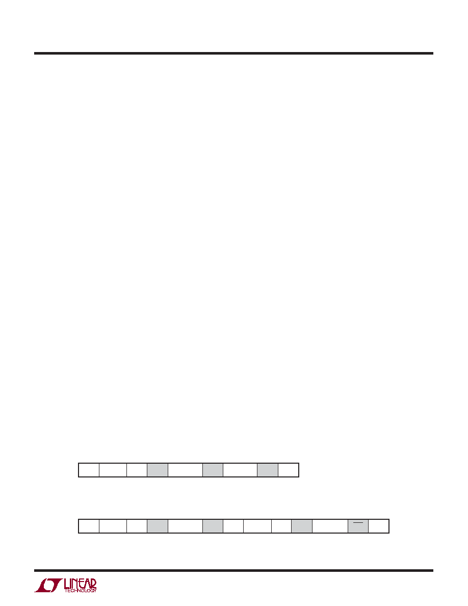
START
WRITE BYTE PROTOCOL
AA01011
XXXXXAAA
WR
ACK
ACK
ACK
STOP
1
1
S
DATA
BYTE
REGISTER
ADDRESS
SLAVE
ADDRESS
0
1
S
0
1
S
0
1
7
1
0
8
8
DDDDDDDD
START
READ BYTE PROTOCOL
AA01011
XXXXXAAA
WR
ACK
ACK
ACK
STOP
1
1
M
3445 G07
DATA
BYTE
REGISTER
ADDRESS
SLAVE
ADDRESS
SLAVE
ADDRESS
1
1
S
0
1
S
0
1
7
1
START
AA01011
1
7
0
RD
ACK
1
S
0
1
1
8
8
DDDDDDDD

16
LTC3445
3445fa
1
2
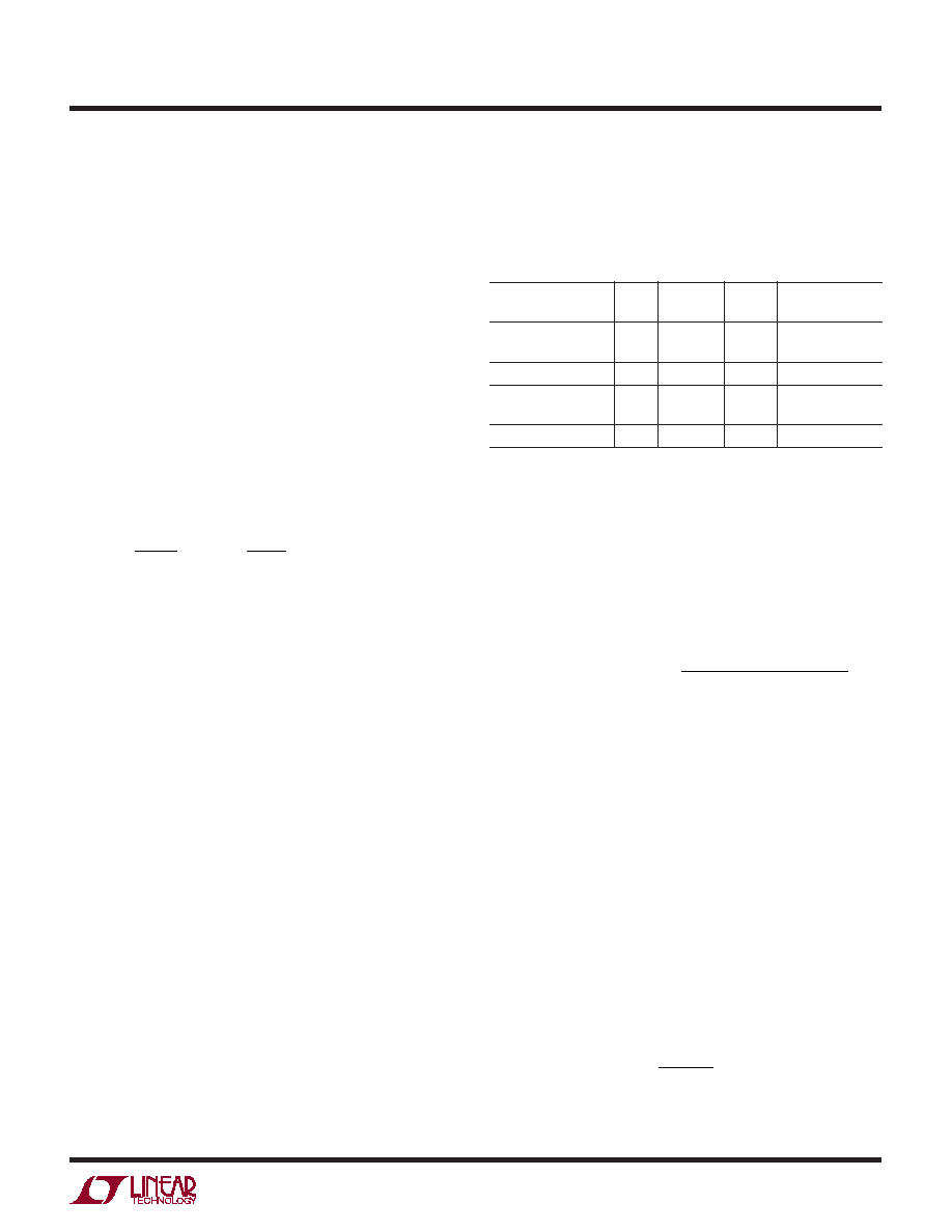
C Register Definitions
(POR = 00 for all registers)
REG 0
REG 1
7
0 (Logic Low)
7
0 (Logic Low)
6
0 (Logic Low)
6
0 (Logic Low)
5
Buck DAC5
5
0 (Logic Low)
4
Buck DAC4
4
0 (Logic Low)
3
Buck DAC3
3
0 (Logic Low)
2
Buck DAC2
2
0 (Logic Low)
1
Buck DAC1
1
Slew Rate 1
0
Buck DAC0
0
Slew Rate 0
REG 2
REG 3
7
0 (Logic Low)
7
PGOOD Blank Disable
6
0 (Logic Low)
6
0 (Logic Low)
5
0 (Logic Low)
5
0 (Logic Low)
4
STATUS--Buck Thermal Shutdown
4
0 (Logic Low)
3
STATUS--Buck PGOODb
3
BURST Mode
2
STATUS--LDO2 PGOODb
2
LDO2 Disable
1
STATUS--LDO1 PGOODb
1
LDO1 Disable
0
Buck Update (GO Bit)
0
Buck Disable
OPERATIO
U
(refer to Figure 1)
REG 5
7
0 (Logic Low)
6
% SPR1
5
% SPR0
4
(Logic Low)
3
(Logic Low)
2
(Logic Low)
1
(Logic Low)
0
(Logic Low)
data line is also left high by the slave and master after a
slave has transmitted a byte of data to the master in a read
operation, but this is a not-acknowledge that indicates that
the data transfer is successful.
Commands Supported
The LTC3445 supports read byte and write byte com-
mands. For the ACK bits, an S indicates that the slave is
pulling the data line low and an M indicates that the master
is effectively acknowledging by leaving the data line high.
Data Transfer Timing for Write Commands
In order to help assure that bad data is not written into the
part, data from a write command is only stored after a
valid acknowledge has been performed. The part will
detect that SDA is low on the rising edge of SCL that marks
the end of the period in which the LTC3445 acknowledges
the data write and then latch the data during the following
SCL low period.
17
LTC3445
3445fa
APPLICATIO S I FOR ATIO
W
U
U
U
BUCK REGULATOR
The basic LTC3445 application circuit is shown on the first
page of this data sheet. External component selection is
driven by the load requirement and begins with the selec-
tion of L followed by C
IN
and C
OUT
.
Inductor Selection
For most applications, the value of the inductor will fall in
the range of 1
µH to 4.7µH. Its value is chosen based on the
desired ripple current. Large value inductors lower ripple
current and small value inductors result in higher ripple
currents. Higher V
CC1
or lower V
OUT
also increases the
ripple current as shown in Equation 1. A reasonable
starting point for setting ripple current is
I
L
= 240mA
(40% of 600mA).
=
( )( )
I
f L
V
V
V
L
OUT
OUT
CC
1
1
1
≠
(1)
The DC current rating of the inductor should be at least
equal to the maximum load current plus half the ripple
current to prevent core saturation. Thus, a 720mA rated
inductor should be enough for most applications (600mA
+ 120mA). For better efficiency, choose a low DC-resis-
tance inductor.
The inductor value also has an effect on Burst Mode
operation. The transition to low current operation begins
when the inductor current peaks fall to approximately
200mA. Lower inductor values (higher
I
L
) will cause this
to occur at lower load currents, which can cause a dip in
efficiency in the upper range of low current operation. In
Burst Mode operation, lower inductance values will cause
the burst frequency to increase.
Inductor Core Selection
Different core materials and shapes will change the size/
current and price/current relationship of an inductor.
Toroid or shielded pot cores in ferrite or permalloy mate-
rials are small and don't radiate much energy, but gener-
ally cost more than powdered iron core inductors with
similar electrical characteristics. The choice of which style
inductor to use often depends more on the price vs size
requirements and any radiated field/EMI requirements
than on what the LTC3445 requires to operate. Table 1
shows some typical surface mount inductors that work
well in LTC3445 applications.
Table 1
MANUFACTURER
VALUE
DCR
MAX DC
SIZE
PART NUMBER
(
µH) (m MAX)
(A)
L
◊ W ◊ H (mm
3
)
Sumida CDRH3D16/
2.2
72
1.2
4.0
◊ 4.0 ◊ 1.8
HP2R2
Sumida CR434R7
4.7
109
1.15
4.0
◊ 4.5 ◊ 3.5
TDK TDK7030T-
2.2
12
5.5
7.3
◊ 6.8 ◊ 3.2
2R2M5R4
Coilcraft D03316P-222
2.2
12
7
12.45
◊ 9.4 ◊ 5.21
C
IN
and C
OUT
Selection
In continuous mode, the source current of the top MOSFET
is a square wave of duty cycle V
OUT
/V
CC1
. To prevent large
voltage transients, a low ESR input capacitor sized for the
maximum RMS current must be used. The maximum
RMS capacitor current is given by:
C
I
V
V
V
V
IN
OMAX
OUT
CC
OUT
CC
required I
RMS
(
)
[
]
1
1 2
1
≠
/
(2)
This formula has a maximum at V
CC1
= 2V
OUT
, where I
RMS
= I
OUT
/2. This simple worst-case condition is commonly
used for design because even significant deviations do not
offer much relief. Note that the capacitor manufacturer's
ripple current ratings are often based on 2000 hours of life.
This makes it advisable to further derate the capacitor, or
choose a capacitor rated at a higher temperature than
required. Always consult the manufacturer if there is any
question.
The selection of C
OUT
is driven by the required effective
series resistance (ESR). Typically, once the ESR require-
ment for C
OUT
has been met, the RMS current rating
generally far exceeds the I
RIPPLE(P-P)
requirement. The
output ripple
V
OUT
is determined by:
+
V
I ESR
fC
OUT
L
OUT
1
8
(3)

18
LTC3445
3445fa
where f = operating frequency, C
OUT
= output capacitance
and
I
L
= ripple current in the inductor. For a fixed output
voltage, the output ripple is highest at maximum input
voltage since
I
L
increases with input voltage.
Aluminum electrolytic and dry tantalum capacitors are
both available in surface mount configurations. In the case
of tantalum, it is critical that the capacitors are surge tested
for use in switching power supplies. An excellent choice is
the AVX TPS series of surface mount tantalum. These are
specially constructed and tested for low ESR so they give
the lowest ESR for a given volume. Other capacitor types
include Sanyo POSCAP, Kemet T510 and T495 series, and
Sprague 593D and 595D series. Consult the manufacturer
for other specific recommendations.
Using Ceramic Input and Output Capacitors
Higher values, lower cost ceramic capacitors are now
becoming available in smaller case sizes. Their high ripple
current, high voltage rating and low ESR make them ideal
for switching regulator applications. Because the
LTC3445's control loop does not depend on the output
capacitor's ESR for stable operation, ceramic capacitors
can be used freely to achieve very low output ripple and
small circuit size.
However, care must be taken when ceramic capacitors are
used at the input and the output. When a ceramic capacitor
is used at the input and the power is supplied by a wall
adapter through long wires, a load step at the output can
induce ringing at the input, V
CC1
. At best, this ringing can
couple to the output and be mistaken as loop instability. At
worst, a sudden inrush of current through the long wires
can potentially cause a voltage spike at V
CC1
, large enough
to damage the part.
When choosing the input and output ceramic capacitors,
choose the X5R or X7R dielectric formulations. These
dielectrics have the best temperature and voltage charac-
teristics of all the ceramics for a given value and size.
Buck Output Voltage Programming
The LTC3445 has an internal resistor divider network tied
to the FB pin. The output voltage is controlled by a DAC
(6-bit register) whose setting is controlled by the I
2
C
interface. The effective DAC bit range is from 0 to 48. Note
that any DAC settings above 48 defaults to the 48 setting.
The DAC controls the V
OUT
range of 0.85V to 1.55V in
~15mV steps. The default value for V
OUT
is 1.35V and is
reset to this value whenever V
CC1
comes up.
When the DAC's value is changed, LTC3445 controls
V
OUT
's slew rate via a 2-bit RATE register. The RATE
register can be updated via the I
2
C interface. The slew rate
can be set to approximately 0.9mV/
µs, 3.8mV/µs, 7.5mV/µs
or 11.3mV/
µs. The default value for RATE is 10mV/µs and
is reset to this value whenever V
CC1
comes up.
The DAC and RATE values are not lost whenever the RUN
pin is deasserted.
Once the DAC and RATE registers are programmed, a GO
bit transition is required for the buck to update. This is
accomplished by changing the GO bit (REG2[0]) from
logic low to a logic high.
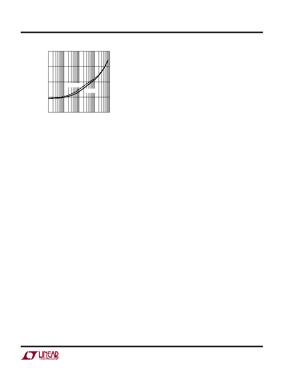
Efficiency Considerations
The efficiency of a switching regulator is equal to the
output power divided by the input power times 100%. It is
often useful to analyze individual losses to determine what
is limiting the efficiency and which change would produce
the most improvement. Efficiency can be expressed as:
Efficiency = 100% ≠ (L1 + L2 + L3 + ...)
where L1, L2, etc. are the individual losses as a percentage
of input power.
Although all dissipative elements in the circuit produce
losses, two main sources usually account for most of the
losses in LTC3445 buck regulator circuits: V
CC1
quiescent
current and I
2
R losses. The V
CC1
quiescent current loss
dominates the efficiency loss at very low load currents
whereas the I
2
R loss dominates the efficiency loss at
medium to high load currents. In a typical efficiency plot,
the efficiency curve at very low load currents can be
misleading since the actual power lost is of no conse-
quence as illustrated in Figure 8.
1. The V
CC1
quiescent current is due to two components:
the DC bias current as given in the Electrical Character-
istics and the internal main switch and synchronous
switch gate charge currents. The gate charge current
results from switching the gate capacitance of the
APPLICATIO S I FOR ATIO
W
U
U
U
19
LTC3445
3445fa
Checking Transient Response
The regulator loop response can be checked by looking at
the load transient response. Switching regulators take
several cycles to respond to a step in load current. When
a load step occurs, V
OUT
immediately shifts by an amount
equal to (
I
LOAD
∑ ESR), where ESR is the effective series
resistance of C
OUT
.
I
LOAD
also begins to charge or
discharge C
OUT
, which generates a feedback error signal.
The regulator loop then acts to return V
OUT
to its steady-
state value. During this recovery time V
OUT
can be moni-
tored for overshoot or ringing that would indicate a stability
problem. For a detailed explanation of switching control
loop theory, see Application Note 76.
A second, more severe transient is caused by switching in
loads with large (>1
µF) supply bypass capacitors. The
discharged bypass capacitors are effectively put in parallel
with C
OUT
, causing a rapid drop in V
OUT
. No regulator can
deliver enough current to prevent this problem if the load
switch resistance is low and it is driven quickly. The only
solution is to limit the rise time of the switch drive so that
the load rise time is limited to approximately (25 ∑ C
LOAD
).
Thus, a 10
µF capacitor charging to 3.3V would require a
250
µs rise time, limiting the charging current to about
130mA.
LDO REGULATORS
The LDOs in the LTC3445 are 50mA low dropout regula-
tors with low quiescent and shutdown currents. Each
device is capable of supplying 50mA at a dropout voltage
of 300mV. The LDOs are current limited to greater than
50mA but less than 75mA. The output voltages of the
LDOs are set with external resistive dividers according to
the following formula:
V
LDOOUT1
= 0.6(1 + R1/R2)
(4)
V
LDOOUT2
= 0.6(1 + R3/R4)
(5)
Output Capacitance and Transient Response
The LTC3445 LDOs are designed to be stable with a wide
range of output capacitors. A minimum output capacitor
of 2.2
µF with an ESR of 3 or less is recommended to
internal power MOSFET switches. Each time the gate is
switched from high to low to high again, a packet of
charge, dQ, moves from V
CC1
to ground. The resulting
dQ/dt is the current out of V
CC1
that is typically larger
than the DC bias current. In continuous mode, I
GATECHG
= f(Q
T
+ Q
B
) where Q
T
and Q
B
are the gate charges of the
internal top and bottom switches. Both the DC bias and
gate charge losses are proportional to V
CC1
and thus
their effects will be more pronounced at higher supply
voltages.
2. I
2
R losses are calculated from the resistances of the
internal switches, R
SW
, and external inductor R
L
. In
continuous mode, the average output current flowing
through inductor L is "chopped" between the main
switch and the synchronous switch. Thus, the series
resistance looking into the SW pin is a function of both
top and bottom MOSFET R
DS(ON)
and the duty cycle
(DC) as follows:
R
SW
= (R
DS(ON)TOP
)(DC) + (R
DS(ON)BOT
)(1 ≠ DC)
The R
DS(ON)
for both the top and bottom MOSFETs can
be obtained from the Typical Performance Charateristics
curves. Thus, to obtain I
2
R losses, simply add R
SW
to
R
L
and multiply the result by the square of the average
output current.
Other losses including C
IN
and C
OUT
ESR dissipative
losses and inductor core losses generally account for
less than 2% total additional loss.
APPLICATIO S I FOR ATIO
W
U
U
U
Figure 8. Power Loss vs Load Current, V
CC1
= 3.6V
LOAD CURRENT (mA)
1
POWER LOSS (mW)
10
100
1000
0.1
10
100
1000
3445 F08
0.1
1
DAC MIN
DAC MAX

20
LTC3445
3445fa
prevent oscillations. The LTC3445 LDOs are micropower
devices and output transient response will be a function of
output capacitance. Larger values of output capacitance
decrease the peak deviations and provide improved tran-
sient response for larger load current changes.
PowerPath CONTROLLER
The PowerPath circuitry in the LTC3445 is used to provide
backup power from V
BACKUP
to the V
CC
BATT pin when
V
CC1
is low or disconnected. When V
CC1
is below 2.8V, the
PowerPath routes V
BACKUP
, typically a coin cell, to the V
CC
BATT pin. While V
BACKUP
is selected there is no current
limiting except for a small (<5
) resistance from the
V
BACKUP
input to the V
CC
BATT output. The LTC3445 sinks
less than 6.5
µA from V
BACKUP
when it is selected and sinks
less than 0.1
µA from V
BACKUP
when it is not selected.
When V
CC1
exceeds 2.8V, V
BACKUP
is disconnected from
V
CC
BATT and an internal LDO regulates the V
CC
BATT
voltage to the minimum of V
CC1
or typically 3V. The
internal LDO is current limited to less than 50mA, but
greater than 10mA. Capacitance on the V
CC
BATT pin
should be at least 2
µF with an ESR less than 3.
V
BACKUP
will be routed to the V
CC
BATT output when the
main battery voltage falls below 2.4V. As the main battery,
V
CC1
, voltage drops from 3V to 2.4V, the LDO will be in
dropout, V
CC
BATT will follow V
CC1
down, rebounding to
V
BACKUP
when V
CC1
falls below 2.4V. If V
CC1
is removed
quickly, the capacitor on V
CC
BATT will limit the V
CC
BATT
droop until V
BACKUP
is switched in.
The V
TRACK
input offers the capability of the V
CC
BATT
voltage to follow the voltage on V
TRACK
up to V
CC1
. In
effect, V
TRACK
overrides the internal reference of the LDO,
resulting in the LDO output (V
CC
BATT) having a gain of 1
relative to V
TRACK
once V
TRACK
exceeds a typical value of
3V. V
CC
BATT will follow V
TRACK
to within 200mV provid-
ing V
TRACK
does not exceed the dropout voltage of the
LDO, which is powered by V
CC1
.
V
BACKUP
should be present prior to V
CC1
being connected.
V
BACKUP
provides power to the BATTFAULT driver which
APPLICATIO S I FOR ATIO
W
U
U
U
is used to detect an absent or low V
CC1
. If V
BACKUP
is not
present, the LTC3445 will be unable to pull the BATTFAULT
pin low to signal a V
CC1
fault condition.
Output Capacitance and Transient Response
The LDO used LTC3445 PowerPath is designed to be
stable with a wide range of output capacitors. A minimum
output capacitor of 2.2
µF with an ESR of 3 or less is
recommended to prevent oscillations. The LTC3445
PowerPath LDO is a micropower device and output tran-
sient response will be a function of output capacitance.
Larger values of output capacitance decrease the peak
deviations and provide improved transient response for
larger load current changes.
THERMAL CONSIDERATIONS
In most applications the LTC3445 does not dissipate
much heat due to its high efficiency. But, in applications
where the LTC3445 is running at high ambient tempera-
ture with low supply voltage and high duty cycles, such as
in dropout, the heat dissipated may exceed the maximum
junction temperature of the part. If the junction tempera-
ture reaches approximately 150
∞C, both power switches
will be turned off and the SW node will become high
impedance. The remaining regulators will also turn off.
To ensure the LTC3445 doesn't exceed the maximum
junction temperature, the user will need to do some
thermal analysis. The goal of the thermal analysis is to
determine whether the power dissipated exceeds the
maximum junction temperature of the part. The tempera-
ture rise is given by:
T
R
=
JA
∑ (PD
BUCK
+ PD
LDO1
+ PD
LDO2
+ PD
PowerPath
)
where P
D
is the power dissipated by the regulator and
JA
is the thermal resistance from the junction of the die to the
ambient temperature.
The junction temperature, T
J
, is given by:
T
J
= T
A
+ T
R
where T
A
is the ambient temperature.
21
LTC3445
3445fa
As an example, consider the LTC3445 in dropout at an
input voltage of 2.7V, an ambient temperature of 70
∞C, a
buck load current of 600mA, LDO1 set to 1.3V with a load
of 25mA, LDO2 set to 1.1V with a load of 15mA, and the
PowerPath regulator at 2.5V with a load of 6
µA. From the
typical performance graph of switch resistance, the R
DS(ON)
of the P-channel switch at 70
∞C is approximately 0.52.
Therefore, power dissipated by the part is:
P
D(BUCK)
= I
LOAD
2
∑ R
DS(ON)
= 180mW
P
D(LDO1)
= (2.7 ≠ 1.3)V ∑ 0.025A = 35mW
P
D(LDO2)
= (2.7 ≠ 1.1)V ∑ 0.015A = 24mW
P
D(PowerPath)
= (2.7 ≠ 2.5)V ∑ 6
µA = 1.2µW
P
D(TOTAL)
= 0.239W
For the QFN24 package, the
JA
is 37
∞C/W. Thus, the
junction temperature of the regulator is:
T
J
= 70
∞C + (0.239)(37) = 78.8∞C
which is well below the maximum junction temperature of
125
∞C. Note that at higher supply voltages, the junction
temperature is lower due to reduced switch resistance
(R
DS(ON)
).
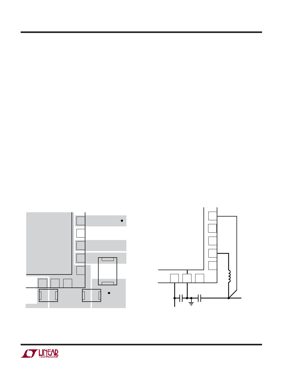
PC BOARD LAYOUT CHECKLIST
When laying out the printed circuit board, the following
checklist should be used to ensure proper operation of the
LTC3445. These items are also illustrated graphically in
Figures 9 and 10. Check the following in your layout:
1. The power traces, consisting of the GND trace, the SW
trace, the V
CC1
trace and the V
CC2
trace should be kept
short, direct and wide.
2. Does the FB pin connect directly to the output voltage
reference? Ensure that there is no load current running
from the reference voltage and the FB pin.
3. Does the (+) plate of C
IN1
connect to V
CC1
as closely as
possible? This capacitor provides the AC current to the
internal power MOSFETs.
4. Keep the switching node, SW, away from the sensitive
FB node.
5. Keep the (≠) plates of C
IN
and C
OUT
as close as possible.
APPLICATIO S I FOR ATIO
W
U
U
U
Figure 9
Figure 10
V
CC1
10
V
CC1
GND
OUT
3445 F09
SW
RUN
FB
GND
25
NC
12
GND
11
NC
13
SW
14
RUN
15
NC
16
VIA TO
OUT
VIA TO
FB
FB
17
C
IN
C
OUT
L1
V
CC1
10
3445 f10
GND
25
L1
V
OUT
BOLD LINES INDICATE HIGH CURRENT PATH
V
CC1
C
IN
NC
12
GND
11
NC
13
SW
14
RUN
15
NC
16
FB
17
C
OUT
22
LTC3445
3445fa
APPLICATIO S I FOR ATIO
W
U
U
U
DESIGN EXAMPLE
As a design example, assume the LTC3445 is used in a
single lithium-ion battery-powered Intel PXA270 micro-
processor application. The battery will be operating from
a maximum of 4.2V down to about 2.7V. Also, the battery
will be connected to all three power pins on the LTC3445.
The desired LDO outputs are 1.3V with a 23mA load and
1.1V with a 14mA load. Since both LDO's are the same, we
will select LDO1 for the 1.3V output and LDO2 for the 1.1V
output. Using Equations 4 and 5, and choosing R2 and R4
to be 604k, the values for R1 and R2 are 705k and 503k
respectively. Also, selecting a 10
µF output capacitor pro-
vides adequate stability and transient reponses.
The PXA270's V
CC
BATT requirement can be readily handled
by the LTC3445's PowerPath control circuits. By simply
connecting a coin cell battery to V
BACKUP
, the PowerPath
control circuits regulate V
CC
BATT within the PXA270's
requirements.
The buck regulator's maximum load requirement for this
application is 300mA. Although the default start-up volt-
age for the buck regulator is 1.35V, ripple current is
greatest when the output voltage is programmed to 0.85V.
For ripple currents of 200mA and the main battery at 4.2V,
the required inductor value is 2.2
µH (Equation 1). For best
efficiency choose a 400mA or greater inductor with less
than 0.3
series resistance. Choosing a 10µF output
capacitor with an ESR of 0.25
will generate a ripple
voltage of 52mV (Equation 3). In most cases, a ceramic
capacitor's ESR will be less than 0.25
further reducing
the output ripple (see Figure 11). Note that as V
CC1
decreases or V
OUT
increases, the ripple current and ripple
voltage will decrease. The input capacitor, C
IN
, will require
an RMS current rating of at least 0.150A
I
LOAD(MAX)
/2 at
temperature (Equation 2).
Figure 11. Design Example
LDO2FB
LDO2
SDA
SCL
1.1V
3445 F11
604k
10
µF
CER
503k
V
CC
_SRAM
LDO1FB
LDO1
FB
SW
1.3V
0.85V TO
1.55V
SUMIDA
CDRH3D16/HP2R2
2.2
µH
604k
3k
3k
10
µF
CER
10
µF
CER
10
µF
CER
705k
3V_TYP
V
TRACK
V
BACKUP
V
CC
V
CC
_PLL
V
CC
_CORE
V
CC
BATT
LTC3445
LTC3406
BUCK
PWR_EN
BATTFAULT
SYS_EN
PGOOD
RUN
V
CC1
V
CC1
V
CC2
ADD7
ADD6
I
2
C BUS
3V
V
CC
_BATT
V
CC
_IO
INTEL PXA270
2.5V TO 5.5V
LITHIUM ION
3V
COIN CELL
nV
CC
_FAULT
20k
V
CC
nBATT_FAULT
20k
23
LTC3445
3445fa
U
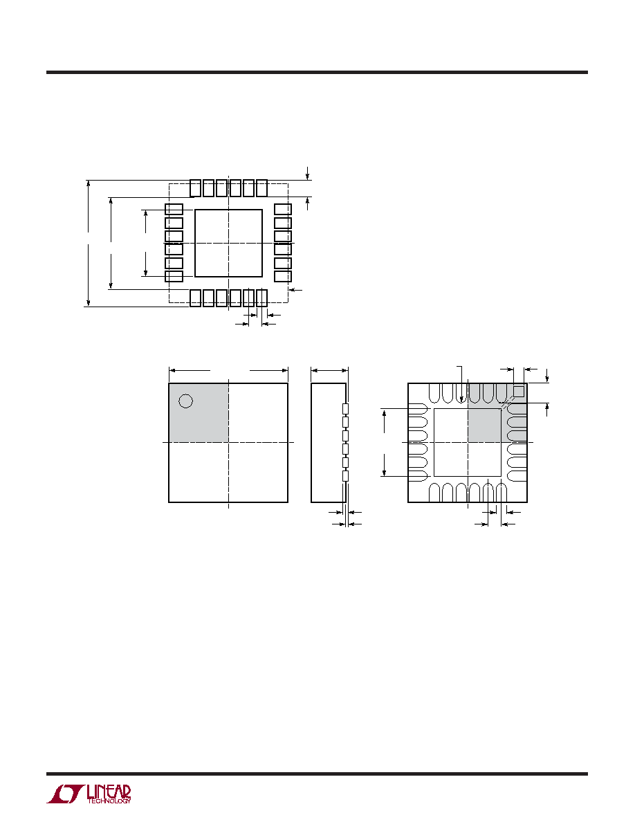
PACKAGE DESCRIPTIO
UF Package
24-Lead Plastic QFN (4mm
◊ 4mm)
(Reference LTC DWG # 05-08-1697)
Information furnished by Linear Technology Corporation is believed to be accurate and reliable.
However, no responsibility is assumed for its use. Linear Technology Corporation makes no represen-
tation that the interconnection of its circuits as described herein will not infringe on existing patent rights.
4.00
± 0.10
(4 SIDES)
NOTE:
1. DRAWING PROPOSED TO BE MADE A JEDEC PACKAGE OUTLINE MO-220 VARIATION (WGGD-X)--TO BE APPROVED
2. DRAWING NOT TO SCALE
3. ALL DIMENSIONS ARE IN MILLIMETERS
4. DIMENSIONS OF EXPOSED PAD ON BOTTOM OF PACKAGE DO NOT INCLUDE
MOLD FLASH. MOLD FLASH, IF PRESENT, SHALL NOT EXCEED 0.15mm ON ANY SIDE, IF PRESENT
5. EXPOSED PAD SHALL BE SOLDER PLATED
6. SHADED AREA IS ONLY A REFERENCE FOR PIN 1 LOCATION
ON THE TOP AND BOTTOM OF PACKAGE
PIN 1
TOP MARK
(NOTE 6)
0.38
± 0.10
24
0.23 TYP
(4 SIDES)
23
1
2
BOTTOM VIEW--EXPOSED PAD
2.45
± 0.10
(4-SIDES)
0.75
± 0.05
R = 0.115
TYP
0.25
± 0.05
0.50 BSC
0.200 REF
0.00 ≠ 0.05
(UF24) QFN 1103
RECOMMENDED SOLDER PAD PITCH AND DIMENSIONS
0.70
±0.05
0.25
±0.05
0.50 BSC
2.45
± 0.05
(4 SIDES)
3.10
± 0.05
4.50
± 0.05
PACKAGE OUTLINE
24
LTC3445
3445fa
© LINEAR TECHNOLOGY CORPORATION 2004
LT/LT 0705 REV A ∑ PRINTED IN THE USA
PART NUMBER
DESCRIPTION
COMMENTS
LT1761
100mA, Low Noise Micropower, LDO
V
IN
: 1.8V to 20V, V
OUT(MIN)
= 1.22V, Dropout Voltage = 0.30V,
I
Q
= 20
µA, I
SD
< 1
µA, V
OUT
= Adj, 1.5V, 1.8V, 2V, 2.5V, 2.8V, 3V,
3.3V, 5V, ThinSOT
TM
Package. Low Noise < 20
µV
RMS(P-P)
, Stable
with 1
µF Ceramic Capacitors
LT1762
150mA, Low Noise Micropower, LDO
V
IN
: 1.8V to 20V, V
OUT(MIN)
= 1.22V, Dropout Voltage = 0.30V,
I
Q
= 25
µA, I
SD
< 1
µA, V
OUT
= Adj, 2.5V, 3V, 3.3V, 5V, MS8
Package. Low Noise < 20
µV
RMS(P-P)
LT1763
500mA, Low Noise Micropower, LDO
V
IN
: 1.8V to 20V, V
OUT(MIN)
= 1.22V, Dropout Voltage = 0.30V,
I
Q
= 30
µA, I
SD
< 1
µA, V
OUT
= 1.5V, 1.8V, 2.5V, 3V, 3.3V, 5V, S8
Package. Low Noise < 20
µV
RMS(P-P)
LTC1844
150mA, Very Low Dropout LDO
V
IN
: 6.5V to 1.6V, V
OUT(MIN)
= 1.25V, Dropout Voltage = 0.08V,
I
Q
= 40
µA, I
SD
< 1
µA, V
OUT
= Adj, 1.5V, 1.8V, 2.5V, 2.8V, 3.3V,
ThinSOT Package. Low Noise < 30
µV
RMS(P-P)
, Stable with 1
µF
Ceramic Capacitors
LT1962
300mA, Low Noise Micropower, LDO
V
IN
: 1.8V to 20V, V
OUT(MIN)
= 1.22V, Dropout Voltage = 0.27V,
I
Q
= 30
µA, I
SD
< 1
µA, V
OUT
= 1.5V, 1.8V, 2.5V, 3V, 3.3V, 5V, MS8
Package. Low Noise < 20
µV
RMS(P-P)
LT3020
Low V
IN
(0.9V) Low V
OUT
(0.2V) VLDO
TM
V
IN
: 0.9V to 10V, V
OUT(MIN)
= 0.20V, Dropout Voltage = 0.15V,
I
Q
= 120
µA, I
SD
< 1
µA, V
OUT
= Adj, DFN Package
LTC3405/LTC3405A
300mA (I
OUT
), 1.5MHz Synchronous Step-Down
V
IN
: 2.5V to 5.5V, V
OUT(MIN)
= 0.8V, I
Q
= 20
µA, I
SD
< 1
µA, ThinSOT
DC/DC Converter
Package
LTC3406/LTC3406B
600mA (I
OUT
), 1.5MHz Synchronous Step-Down
V
IN
: 2.5V to 5.5V, V
OUT(MIN)
= 0.6V, I
Q
= 20
µA, I
SD
< 1
µA, ThinSOT
DC/DC Converter
Package
LTC3407
Dual 600mA, 1.5MHz Synchronous Step-Down
V
IN
: 2.5V to 5.5V, V
OUT(MIN)
= 0.6V, I
Q
= 40
µA, I
SD
< 1
µA, MS10E
DC/DC Converter
Package
LTC3411
1.25A (I
OUT
), 4MHz Synchronous Step-Down
V
IN
: 2.5V to 5.5V, V
OUT(MIN)
= 0.8V, I
Q
= 60
µA, I
SD
< 1
µA, MS10
DC/DC Converter
Package
LTC3412
2.5A (I
OUT
), 4MHz Synchronous Step-Down
V
IN
: 2.5V to 5.5V, V
OUT(MIN)
= 0.8V, I
Q
= 60
µA, I
SD
< 1
µA,
DC/DC Converter
TSSOP16E Package
LTC3455
Dual DC/DC Converter with USB Power Manager and
V
IN
: 3V to 5.5V, Seamless Transition Between Input Sources and
Li-Ion Battery Charger
Li-Ion Battery, USB, 5V Wall Adapter, QFN24 Package
LTC4055
USB Power Manager and Li-Ion Battery Charger
Standalone Charger, Automatic Switchover when Input Supply
is Removed
LTC4411/LTC4412
PowerPath Controllers in ThinSOT
More Efficient than Diode ORing
ThinSOT and VLDO are trademarks of Linear Technology Corporation.
RELATED PARTS
Linear Technology Corporation
1630 McCarthy Blvd., Milpitas, CA 95035-7417
(408) 432-1900
FAX: (408) 434-0507
www.linear.com